Gorilla Flow Reviews
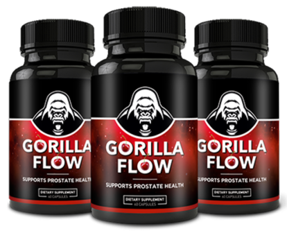
Gorilla Flow Reviews [Updated] – Gorilla Flow is a nutritional supplement that aids men with urinary problems, BPH, and prostate-related problems. Learn More! Official Website: Click Here Do you have troubles with your prostate or your urinary system? Then you’ll find our Gorilla Flow review to be helpful. Many people nowadays are dealing with prostate-related … Read more